India just unveiled its first space-grade microprocessor VIKRAM3201 at Semicon India 2025. With SLTL laser tech driving chip precision, the trillion-dollar semiconductor race is heating up, don’t get left behind in this revolution!
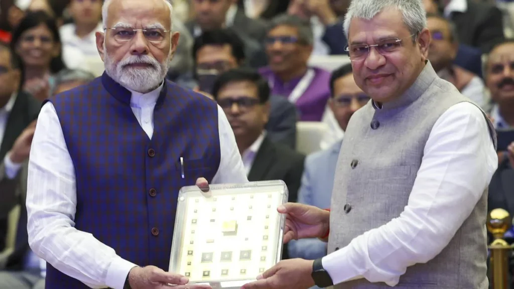
The semiconductor industry stands as the backbone of modern technology, powering everything from smartphones and electric vehicles to satellites and AI-driven devices. On September 2, 2025, India marked a defining moment in its journey to become a semiconductor powerhouse. At Semicon India 2025, held at Yashobhoomi, New Delhi, Prime Minister Narendra Modi was presented with the first ‘Made in India’ Launch Vehicle Grade Microprocessor – the VIKRAM3201, developed by ISRO’s Vikram Sarabhai Space Centre and the Semiconductor Laboratory (SCL), Chandigarh.
Union IT Minister Ashwini Vaishnaw, who presented the chip to the Prime Minister, also handed him a memento containing 31 prototype chips designed by India’s leading academic institutions, including IIT Roorkee, IIT Jammu, IIT Dhanbad, IIT Ropar, NIT Durgapur, and NIT Calicut, among others. These prototypes represent India’s expanding research and innovation ecosystem in semiconductors, laying a strong foundation for future chip design and manufacturing.
India’s Semiconductor Mission: Building the Next Powerhouse
With the theme “Building the Next Semiconductor Powerhouse”, Semicon India 2025 highlighted the progress made under the India Semiconductor Mission (ISM). Minister Vaishnaw noted that within just three and a half years since ISM’s launch, India has gained the world’s confidence.
Key developments include:
- Five semiconductor units currently under construction.
- A pilot line already completed at one unit.
- Two more fabs expected to start production in the coming months.
These advancements signal that India is moving beyond vision into execution mode, establishing the foundation of a trillion-dollar semiconductor industry. Stable policies, skill development, and academic-industry collaborations are attracting global players to India’s growing semiconductor ecosystem.
Why Laser Technology is Crucial for Semiconductors
While India’s semiconductor ambitions gain momentum, success ultimately depends on manufacturing precision. Semiconductors require processes that function at micron and sub-micron scales. Conventional tools are inadequate for the fragile nature of wafers, ICs, and MEMS.
Here, laser technology becomes indispensable:
- Laser Cutting: Precise wafer dicing and scribing with burr-free, crack-free results.
- Laser Marking: Permanent, high-contrast IDs and QR codes for global traceability.
- Laser Welding: Airtight, hermetic sealing of microchips and sensor packages to safeguard against contamination.
- Micro-Machining: Sub-micron structuring for MEMS, cooling channels, and optical components.
Lasers are uniquely suited for this industry because they are:
- Thin: Capable of working on ultra-thin wafers without causing cracks or breakage.
- Precise: Delivering micron-level accuracy for critical chip features.
- Versatile: Adaptable for cutting, welding, marking, cleaning, and drilling across multiple materials.
- Powerful: Concentrated energy beams that achieve results impossible with mechanical tools.
Applications of SLTL Laser Solutions in Semiconductor Manufacturing
- Laser Cutting and Scribing: Semiconductor wafers and substrates must be divided into precise chips. Laser cutting and scribing offer burr-free, crack-free edges while minimizing material loss. This ensures that high-value wafers, such as those used in processors like VIKRAM3201, maintain structural integrity during production.
- Laser Grooving and Dicing: Grooving and dicing are essential for separating chips on a wafer. Laser systems make this process faster, more reliable, and contamination-free compared to blade-based techniques. The precision of lasers ensures consistency even on ultra-thin wafers used in advanced microelectronics.
- Laser Welding: Packaging is critical in protecting delicate semiconductor devices. Laser welding provides hermetic sealing of chip enclosures and sensors, ensuring durability against moisture, dust, and temperature extremes. This is especially vital for mission-critical applications, such as space-grade processors and defense electronics.
- Laser Marking: Every semiconductor component must be traceable in global supply chains. Laser marking allows permanent, high-contrast marking of QR codes, batch IDs, and serial numbers on wafers, ICs, and PCBs. Since it is a non-contact process, it does not affect the electrical properties of the chip.
- Coating Removal and Laser Cleaning: Many semiconductor components involve coatings for protection or functionality. Laser cleaning removes unwanted coatings and residues with pinpoint accuracy, avoiding damage to the substrate. This is also critical during refurbishment or quality-control processes.
- Laser Drilling: Advanced chips and sensors often require micro-holes and channels for cooling, fluidics, or MEMS applications. Laser drilling offers unmatched accuracy and repeatability for these intricate features.
SLTL’s Role in Powering Semiconductor Manufacturing
As a leader in advanced laser solutions, SLTL Group provides end-to-end technologies tailored for the semiconductor industry:
- Accurate slicing of silicon wafers used in chips like VIKRAM3201.
- Prevents micro-cracks, ensuring device reliability in high-stress environments such as space missions.
- Permanent micro-markings on ICs and PCBs.
- Critical for global supply chains, ensuring compliance and authenticity.
- Delivers strong, contamination-free seals to protect sensitive electronics.
- Essential for applications in ISRO avionics and next-gen consumer electronics.
- Enabling cooling systems, MEMS, and optical sensors.
- Aligns with academic research outputs like the 31 prototype chips from IITs and NITs.
By integrating IoT and automation, SLTL ensures that semiconductor manufacturers not only achieve unmatched precision but also align with Industry 4.0 standards.
Advanced Laser Drilling for Multilayer Printed Antennas
Beyond wafer processing and chip packaging, SLTL also plays a vital role in enabling complex semiconductor-driven systems such as multilayer printed antennas, widely used in aerospace, satellite communication, and defense technologies.
SLTL’s 11-axis high-speed drilling and alignment system is specifically engineered for extreme precision in fabricating these multilayer antenna structures. The process involves:
- Pick, place, and align ultra-thin layers of specialized materials.
- Laser drilling with micron-level accuracy to create vias and interconnects.
- Inspection at every stage to ensure reliability and consistency.
This capability is crucial in the assembly of high-frequency communication antennas, where even the smallest deviation can impact performance in satellites and space missions. By providing such precision laser drilling solutions, SLTL extends its expertise beyond chip-level processes into the broader semiconductor ecosystem, reinforcing its role as a trusted partner in India’s advanced technology and space programs.
Shaping India’s Semiconductor Future
The VIKRAM3201 microprocessor and the academic-led prototypes presented at Semicon India 2025 symbolize India’s determination to lead in chip design, fabrication, and innovation. With five fabs under development, stable government policies, and growing global confidence, India is poised to be a key player in the $1-trillion semiconductor market.
But the heart of this revolution lies in precision-driven manufacturing. That’s where SLTL’s laser cutting, marking, welding, and cleaning solutions empower semiconductor fabs, research labs, and industries – enabling India to deliver chips that are reliable, scalable, and future-ready.
From space-grade processors like VIKRAM3201 to everyday electronics, SLTL is committed to shaping the future of semiconductors with laser brilliance.
Author Bio

Mayank Patel
R&D HeadMayank Patel is the Head of Research & Development at SLTL Group, bringing over 20+ years of hands-on experience in the field of laser technology. A forward-thinking innovator, he has played a pivotal role in developing advanced laser cutting, welding, and marking solutions tailored for diverse industries. Under his leadership, SLTL’s R&D division continues to push the boundaries of what laser systems can achieve in modern manufacturing.